

PCB Basics
1. What is a PCB?
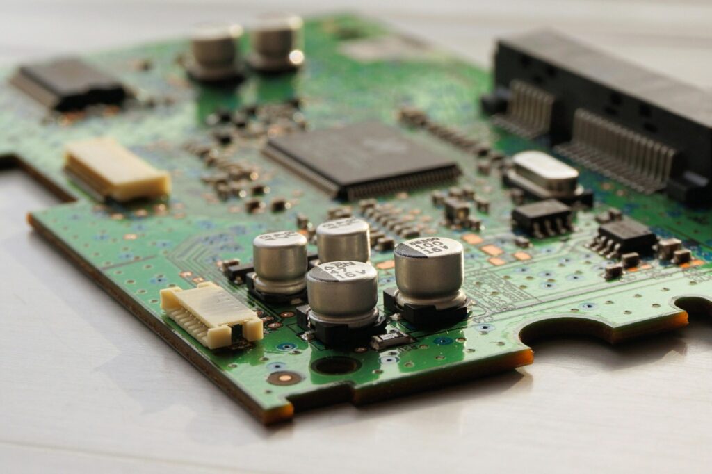
A printed circuit board (PCB) mechanically supports and electrically connects electronic components using conductive pathways, or traces, etched from copper sheets laminated onto a non-conductive substrate.
2. Layers and Materials:
- Single-sided PCBs: Feature copper traces on one side of the board.
- Double-sided PCBs: Have copper traces on both sides of the board, allowing for more complex circuits.
- Multi-layer PCBs: consist of several layers of copper traces separated by insulating material.
3. PCB Design:
The design process includes schematic capture, PCB layout, and generating Gerber files, which are used to fabricate the PCB.
4. Manufacturing Process:
The manufacturing process involves several steps: designing, transferring the design onto the copper-clad board, etching, drilling, plating, solder masking, and finally silkscreen printing.
5. Components and Assembly:
Components are then soldered onto the PCB. This can be done using through-hole or surface mount technology (SMT).
6. Testing:
Testing ensures that the PCB functions correctly before being used in electronic devices.